Above:
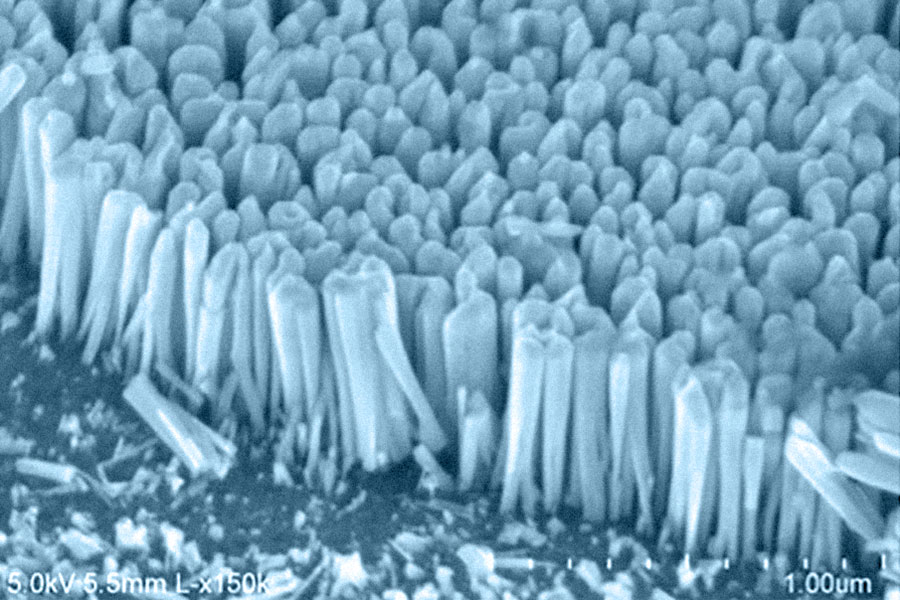
Scanning electron microscope (SEM) image of the nanowire array; each nanowire is about 40-60nm diameter.
Nanowires
Nanowire Detectors
Sarath Gunapala
Modern Earth science, planetary science, and astronomy increasingly depend on large-area focal plane array technology for high spatial resolution. There are a number of approaches being explored to meet this challenge. The new advances in epitaxial growth of III-V semiconductors on silicon could change how we explore the universe, both from the ground and from space.
The use of silicon-based detector array technology in infrared instruments could represent a breakthrough in remote sensing. Prior to this work, monolithic silicon-based infrared detection technology was an elusive goal, mostly due to the inability to grow suitable defect-free light-absorbing semiconductor heterostructures with high quantum efficiency (QE) on silicon.
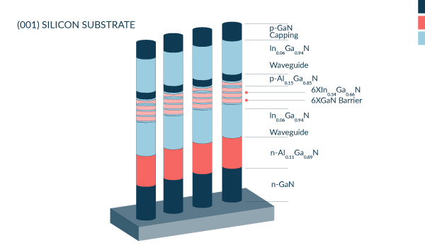
We have been working with Dr. Pallab Bhattacharya, who has pioneered catalyst-free growth of GaN nanowires and InGaN-GaN nanowire heterostructures on (001) silicon substrates. Single or multiple 2–3nm thick InxGa1-xN disks can be inserted in the GaN nanowires. The alloy composition in the disk region can be varied, thereby varying the effective band-gap. It has recently been discovered that quantum dots are formed in the InGaN disk in the nanowires. These quantum dots would be the main photon-absorbing regions in the proposed IR detector. The size and composition of the dots can be varied to tune the interband and intersubband transition energy in the disk (dot), and therefore the wavelength of light absorbed over a wide range. A detector technology using III-nitride nanowires has not been previously demonstrated across a broad range of wavelengths.
Our present work focuses on development of monolithic mid-wavelength and long-wavelength infrared detectors using III-nitride nanowire grown on silicon. We are currently testing performance of these III-nitride nanowire detectors monolithically grown on silicon substrates. Advantages include the elimination of the complex process of In-bump bonding of the detector arrays onto silicon readout integrated circuits (ROICs), performance degradation due to the hybridization process and the associated cost.
This advance will pave the way for demonstration of very large-format infrared focal planes because both the detector arrays and ROICs are based on silicon substrate (i.e., no thermal mismatch issues, no epoxy backfilling). Large-format infrared focal planes are highly relevant to JPL missions and programs for imaging and spectral imaging applications. This effort of III-nitride monolithic nanowire IR detectors on silicon substrates will also enable low-cost, very large FPAs for constellations of low-cost platforms such as CubeSats and SmallSats.