Above:
Detector Array: A scanning electron microscope (SEM) image of a part of a detector array; each square is 20µm x 20µm. Indium bumps have been deposited on the individual delineated detector pixels to facilitate hybridization with silicon readout integrated circuit (ROIC) for imaging focal plane array (FPA) fabrication.
Microlens
Making IR Cameras See Better
Alexander Soibel
Single microlens and microlens arrays operating in the visible and near-infrared spectral bands are well-developed and are utilized in many devices such as smartphone cameras. However, microlens technology in the mid- and long-wavelength infrared spectral bands lags behind. Highly sensitive infrared imagers operating at temperatures accessible with thermoelectric coolers are essential for the next generation of compact instruments for small satellites.
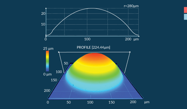
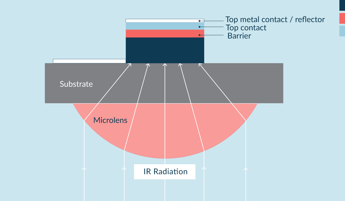
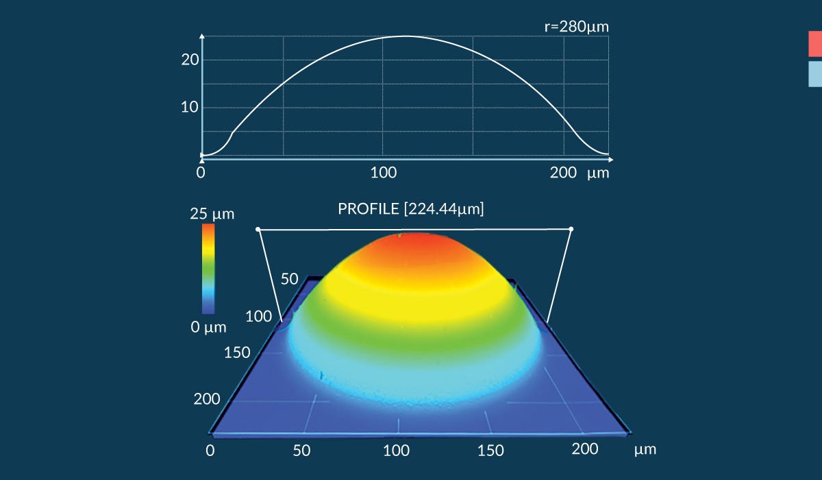
In our most recent work, we increased the sensitivity and operating temperature of nBn detectors by monolithically integrating them with microlenses. These microlenses were fabricated on the backside of the detector wafer. The microlens shape sets the focal length which has to be close to the wafer thickness to optimize light-focusing efficiency.
Microlenses are defined by photoresist reflow and material etching processes that were optimized to achieve the desired microlens shape and focal length. After fabrication of the microlens, the detector’s pixels were fabricated on the front side. Detectors and microlenses were precisely aligned to each other during fabrication. This method negates the time-consuming optical post-alignments of other microlens-detector integration approaches.
The increase in the optical collection area in the detector with an integrated microlens resulted in a five-fold enhancement of the responsivity. These 4.5 µm cut-off wavelength antireflection-coated detectors with microlenses exhibited a detectivity of D* (λ) = 2.7 × 10¹⁰ cmHz0.5/W at T = 250 K, which can be reached easily with a single-stage thermoelectric cooler or with a passive radiator in a space environment. This represents a 25 K increase in the operating temperature of these devices compared to the uncoated detectors without an integrated microlens.
Schematic of the nBn detector with a monolithically integrated microlens. The microlens is fabricated on the backside of the substrate prior to detector fabrication on the front side. The top metal contact serves as a mirror to increase detector responsivity.
+ Larger image
Three-dimensional map of the µlens shape measured with a Zygo interferometric microscope.
+ Larger image

