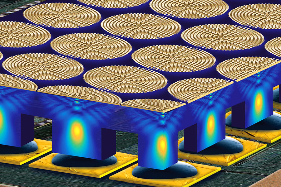
Above:
Infrared detectors monolithically integrated with flat lenses. A new technology utilizing nanostructured flat lenses has the potential to improve infrared sensor performance.
Flat Lens
Flat Lenses Give Better Vision
Alexander Soibel
High operating temperature for detectors can be achieved by using optical concentrators that increase optical collection area while keeping detectors volume constant. The most common type of optical concentrator is a spherical microlens, but this technology is not well developed in mid- and long-wavelength infrared.
The latest is a new class of optical components, dubbed metasurfaces has been developed, based on inhomogeneous arrays of optical resonators with sub-wavelength separation. By accurately designing the properties of each element of the array, the wavefront of scattered or transmitted light can be reshaped and redirected at will depending on the design. The flat lenses are extremely thin, lightweight, and free from spherical aberration when compared with conventional refractive lenses. We are working with a pioneer of flat lens development, Professor Federico Capasso at Harvard University, to extend flat lens technology into mid- and long-wavelength infrared spectral ranges. Our current project focuses on the development of a flat lens covering the 3–5µm spectral band.
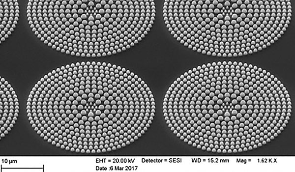
Shown below is a scanning electron microscope (SEM) image of a flat lens designed by the Harvard group, fabricated on GaSb substrate at MDL using electron-beam lithography and dry etching. The lens consists of rods with sub-wavelength diameters varying across its diameter which results in modulation of the transmitted light wavefront and focusing. The lens is 30µm in diameter, and the designed focal length is about 100 µm, which makes it compatible with focal plane array architectures.
We are currently testing performance of these lenses and will monolithically integrate them with single-pixel detectors and focal plane arrays in the near future. Metamaterial flat lens development will greatly benefit instruments for outer planet missions as well as small satellites for Earth observations.
Scanning electron microscope (SEM) image of four flat lenses fabricated on GaSb substrates. The lens diameter is 30 microns and focal length is estimated to be 100 microns.
+ Larger image


