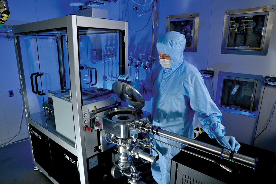
The light that reaches our telescopes from objects in space can be incredibly faint due to distance or low radiance and scientists are continuously searching for better ways to observe these dim signals. Similarly, increasing levels of accuracy are sought for spectrometers and other critical instruments. MDL has been pivotal in advancing the state of the art for such instrumentation through their microfabrication abilities and processes.
Ongoing development of UV, X-ray, infrared, and submillimeter telescopes and spectrometers will revolutionize our understanding of the formation and habitability of the solar system and beyond. While existing technology has allowed us to probe deep into space, materials and fabrication challenges still limit the sensitivity and capability of the detectors and instruments used in these investigations. MDL utilizes the unique precision and control afforded by Atomic Layer Deposition (ALD) to substantially increase the capability of the instruments and detectors that scientists use to make new discoveries.
ALD is a chemical technique that creates devices with control precision and flexibility at the angstrom scale. High-quality, pinhole-free films of a wide variety of materials can be assembled with extreme precision and uniformity over an arbitrarily large surface area. In MDL, ALD films have been employed in the coating, passivation, and fabrication have UV, infrared, and submillimeter detectors. ALD processes also enabled the conformal coating of three-dimensional structures, an extremely challenging process that results in unique materials with excellent strength-to-weight ratios, tailorable surface-free energies (for contamination control on instruments), and metamaterial-like optical properties.
The ability of ALD to coat three-dimensional patterns will enable the synthesis of new types of mechanical and functional nano- and microstructures with unique strength-to-weight ratios and optical properties. ALD is an area of rapid growth at MDL. The ability of ALD to produce novel materials such as nanoalloys uniformly on large substrates could make the precise control and selection of superconducting transition temperature for a given detector more achievable with a wider variety of materials.
In addition, ALD can coat the inside of holes that are tens of microns across and hundreds of microns deep and may ultimately enable MDL engineers to make hybridized superconducting devices with a higher fill factor than current approaches allow. ALD is truly a fabrication process of the future that is occurring today and empowering ever more fruitful missions of Earth observation, planetary science and astrophysics.
Recently, our work in atomic layer deposition has extended beyond what can be achieved solely through thermal or plasma based chemical reactions. Even though a huge variety of materials can be deposited by ALD (metals, oxides, nitrides, fluorides), their properties and their composition are almost always determined by the thermodynamics of the chemicals precursor and the thin film materials themselves. This is a problem of particular concern when attempting to deposit boride compounds, for example, magnesium borides. Stoichometric MgB2 is a high temperature superconductor (~40K) that is useful for a wide variety of devices of great interest to NASA (detectors, mixers, etc.). Conventional chemical vapor deposition (CVD) and ALD techniques with available precursors lead to magnesium deficient compounds such as Mg2B7 which is an insulator.
At JPL, we have invented and are developing a brand new technique called thermal evaporation enhanced atomic layer deposition (TE-ALD). In TE-ALD of MgB2, we integrate a thermal evaporator for magnesium directly into the ALD deposition chamber. An overpressure of magnesium generated by the evaporator is allowed to equilibrate with a growing boron film, which results in ultrathin, layer-by-layer growth of MgB2. This technique may ultimately have applications in a wide variety of other applications, beyond NASA, such as work function control of thin metal nitride films in the semiconductor industry.
Dr. Greer joined JPL in 2007, working in Division 38 in the MDL applying ChemE and semiconductor processing techniques to the fabrication of instrument components to support current and future NASA missions and reimbursable tasks. He currently works on the WFIRST CGI in collaboration with Division 32 and as a PI/CoI on various internally and externally funded R&D tasks to develop new materials and processes for next-generation instruments.
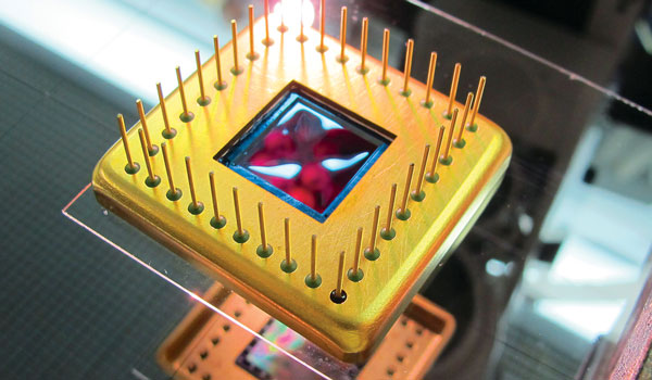
Fully packaged Cassini delta-doped CCD with ALD-deposited anti-reflection coating achieving world-record quantum efficiency in the ultraviolet.
+ Larger image