Above:
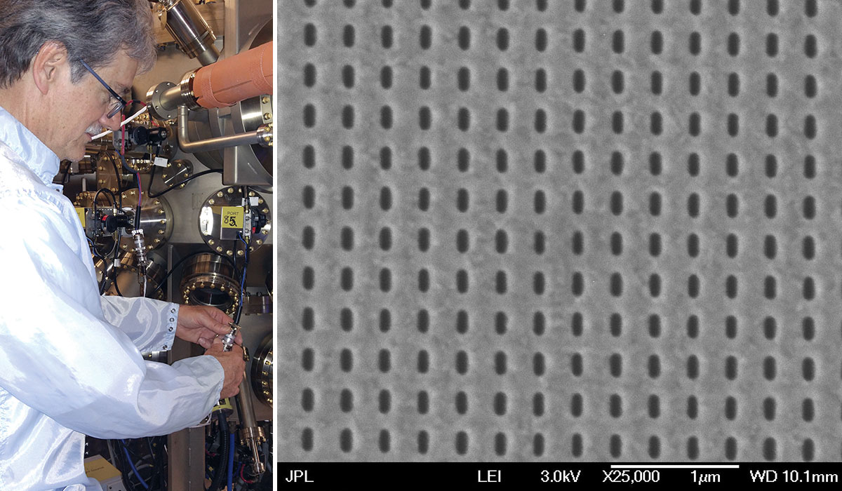
Nanohole arrays patterned into aluminum (inset) can be employed as ultraviolet filtering elements as illustrated by the calculated electric field resonance shown in cross-section for a single hole when illuminated by a particular wavelength. Concepts in plasmonics and metamaterials can potentially be exploited to yield optical components and integrated detector systems that are difficult to accomplish with classical devices and conventional optical materials.


